No information available.
Routing a real 4-layer flight board for $0 of inference
A handover, not a brag: how a small board went from "17 shorts, unusable" to a fab-ready Gerber package without buying a single token of "spatial reasoning".
The assumption I want to argue with
The default answer to "how do I get an AI to route a PCB?" is: use the most expensive model you can afford, because routing is spatial and frontier models are better at space. We tried the variant of that idea — let a large language model emit coordinates — and it produced boards with 17 shorts. Not "suboptimal". Electrically dead.
So we stopped asking a language model to do geometry, and built a referee instead. The result: a 4-layer board with 49/49 vias at the target 0.60 mm / 0.30 mm, zero shorts, zero clearance violations, zero unconnected nets, and an orderable Gerber package — at $0 of inference cost, with the whole campaign measured by one scorecard.
This post is the handover: the toolchain, the three failure modes, the numbers, and the one rule that keeps it honest.
1. The toolchain (all of it free)
| Stage | Tool | Why it is the right tool |
|---|---|---|
| Board read/write, geometry | pcbnew (KiCad's Python API) | exact copper geometry, not a screenshot |
| DRC — the referee | kicad-cli pcb drc --format json | machine-readable violations, per class |
| Autorouting | KRT (KiCadRoutingTools, Rust A*, octilinear, multi-layer, auto-vias) | deterministic, CLI, --refill-zones, placement-for-routability |
| Second opinion router | FreeRouting (Java) via a Specctra DSN round-trip | independent implementation; if two routers disagree, you learn something |
| Schematic/netlist | SKiDL | netlist generated, not typed |
| Measurement | our own drc_score.py | one row per attempt — progress becomes a number, not an opinion |
No model was in the loop for the final board. LLMs were used for review and for writing the tooling around the deterministic core — which is exactly the part they are good at.
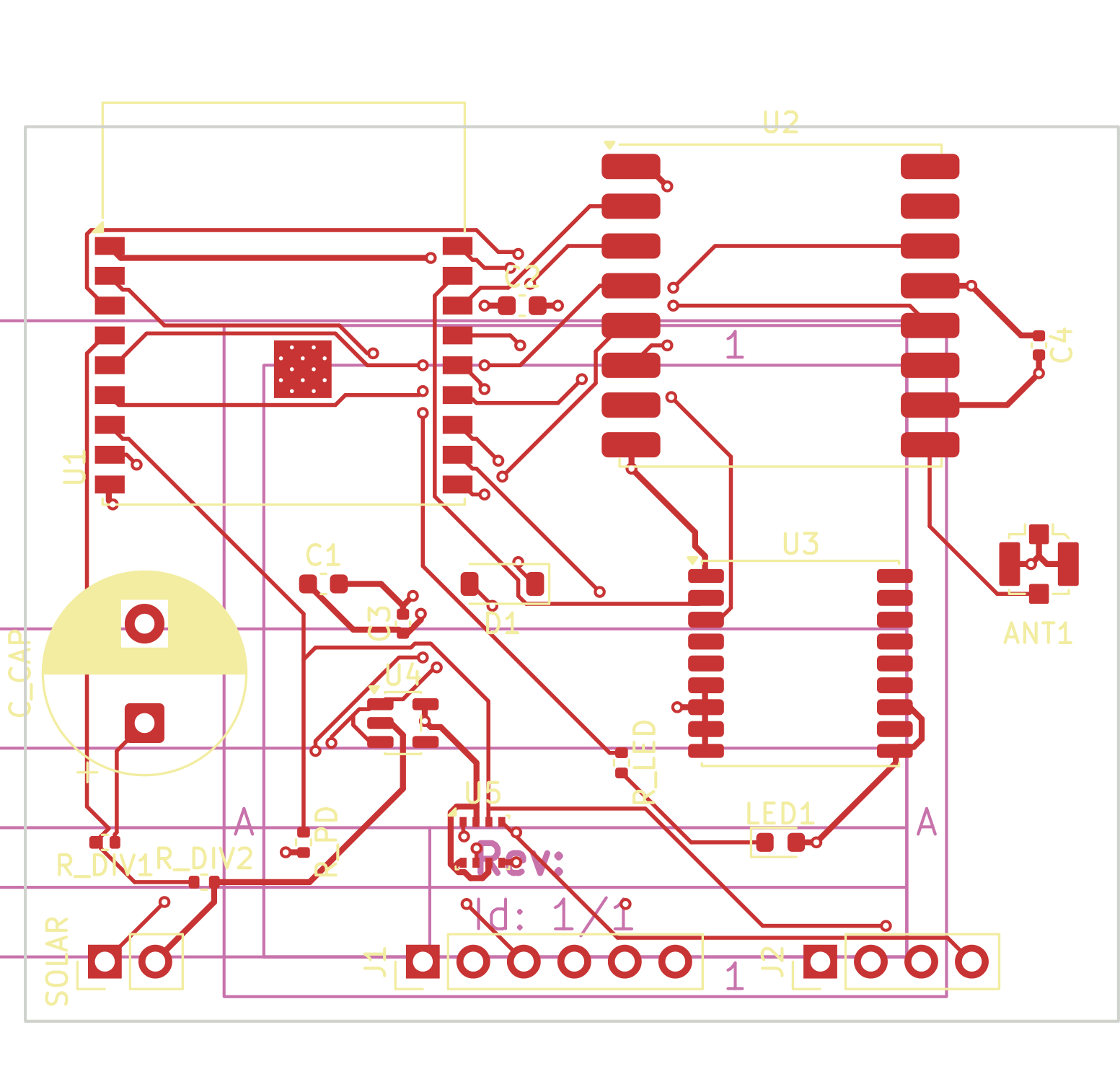
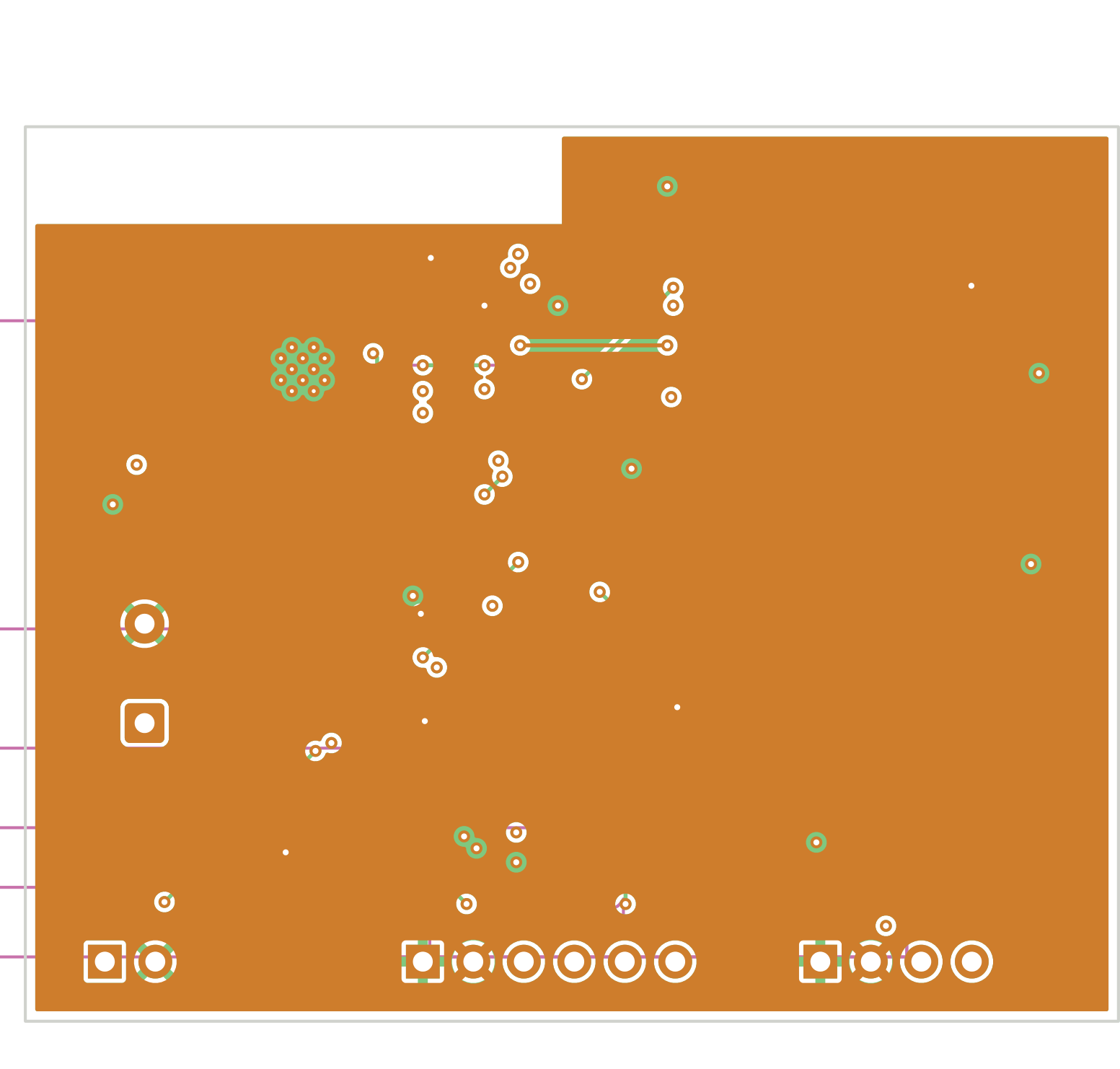
2. The one rule that keeps it honest
Most PCB debugging conversations are unproductive because "clean" is a vibe. Ours is a tuple:
progress  = shorts + clearance + tracks_crossing + unconnected   must FALL
fab-ready = shorts == 0 AND clearance == 0 AND unconnected == 0 AND footprints >= 10
Every routing attempt appends exactly one row to a scorecard (drc_score.py): board path, sha256, tool, cost, violation classes. Cosmetic classes are separated explicitly — silk_edge_clearance, solder_mask_bridge, lib_footprint_mismatch and friends are informational for JLCPCB and never counted as progress.
A restated rule that saved us repeatedly: a commit message saying "DRC clean" is not evidence. One early card claimed exactly that; the actual report had 44 shorting_items. Only the parsed JSON counts.
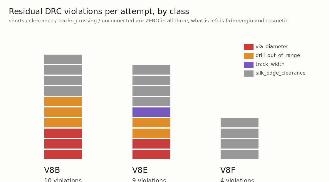
The progression above is the entire argument of this post: 10 → 9 → 4 residual violations, with the electrical classes at zero throughout, and the last four being silkscreen clipped by the board edge.
3. Three failure modes, and what actually fixed them
3.1 Placement caps routing — no router can rescue two parts in one space
The first board failed a placement gate with the same two pad-overlap pairs on a 2-layer route, a 4-layer route and a fully automated route. Identical across three methods means the router was never the problem.
Diagnosis path: rip all tracks, check pad bounding boxes for overlaps, run DRC with zero copper. If the placement fails, stop — routing on top of it only manufactures violations. Fix placement, freeze it (sha256), then route. Board-size increase was cheaper than the debugging: 45×35 mm → 50×40 → 55×45 mm turned "45 overlapping parts" into "all 20 fit with 2 mm gaps".
Rule: placement is a gate, not a phase. Nothing routes until it passes.
3.2 Post-hoc DRC fixing does not converge
Fixing shorting_items after generation is a treadmill: an 86-short board reached 1002 violations after a "fix", and U-shaped detours traded shorts for unconnected nets. The only class that repairs cleanly post-hoc is unconnected (parse → inject a bridge trace). Real violations must be fixed at generation time, which is what the clearance-aware router does: register every pad/via/track as an obstacle and check clearance before placing a segment.
3.3 Via-in-pad: the router quietly downgrades your via size
This is the one that produced the post's headline image. The rule file asked for 0.60 mm vias with 0.30 mm drills — and the router did deliver 48 of 51 that way. The other three came back at 0.45 mm / 0.20 mm, emitted as "via-in-pad clamps" to escape a fine-pitch part, and the process exited with code 3 to say so.
Two things made this hard to see:
--strict-sizesdoes not prevent it. Re-running with that flag produced the same three vias.- The part was a BMP280 (an LGA-8, 2.5 × 2.5 mm, 0.65 mm pitch) that the router's log labelled a "BGA exclusion zone". At 0.65 mm pitch there is ~0.15 mm between pads — no 0.60 mm via fits inside the pad ring, so it did the thing that always "works": put the via in the pad.
Two legitimate ways out, and we did both in sequence:
- Forbid via-in-pad (
--same-net-pad-clearance 0.2). That moved two of the three vias off-pad and left fewer, smaller vias — progress, but not the margin we wanted. - Relocate the survivors with exact geometry — a small script that searches a 0.025 mm grid for a site where a 0.60 mm via keeps its distance, then re-attaches the same tracks to the new position and refills the zones.
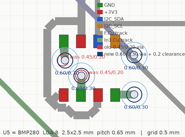
The trap in step 2 is worth its own paragraph, because we walked into it. A relocation pass written earlier in the project moved all three vias to a legal-looking 0.60 mm site, removed every via-size violation — and introduced 4 clearance + 3 hole-clearance violations. It had enforced the 0.20 mm copper-clearance rule and ignored the board's own 0.25 mm copper-to-hole rule. Seven blocking electrical violations in exchange for a fab-margin note: strictly worse, and the scorecard caught it (7 blocking open, not fab-ready).
The fix that worked checked both constraints, plus a 0.5 mm board-edge rule, and added a 0.01 mm safety margin over each rule so a floating-point equality could not fail the DRC:
via (22.700, 36.300) -> legal in place; only the SIZE changed 0.45/0.20 -> 0.60/0.30
via (22.000, 35.700) -> shifted 0.075 mm in x; same size change
zones refilled afterwards  (so the inner +3V3 pour regenerates its antipads for the wider via)
1 track widened 0.1998 -> 0.200 mm  (a rounding artifact, not a routing error)
The 0.075 mm shift is the whole point: the margin was geometry, not intelligence. A grid search over a 7 × 5 mm window found it in seconds, for free, and DRC verified it.
Also learned: after changing a via size, refill the zones. A stale zone fill after an import is the second-most-common phantom violation class we hit, and it looks exactly like a real short.
4. The numbers
| Attempt | Router | Residual violations | Electrical | Vias at target | |---|---|---|---|---| | v8b | FreeRouting-era candidate | 10 | 0 | 48 / 51 | | v8e | KRT, via-in-pad forbidden | 9 | 0 | 47 / 49 | | v8f | v8e + exact-geometry escape fix | 4 | 0 | 49 / 49 |
All three are "fab-ready" by the rule above. v8f is the one that ships: every via at the intended 0.60 mm / 0.30 mm, no via-in-pad at all, and the only residual class is four silkscreen lines clipped by the board edge — cosmetic, ignored by the fab.
Cost: $0.00 inference for all three. Wall-clock: the autoroute is ~1–2 seconds; the escape probe is seconds; DRC is ~1 second; the whole campaign is minutes, plus human review.
The order package is a 136 KB zip: 11 plotted layers, 75 plated holes, a 20-component placement file at top-left origin, and the drill files.
5. What this means for "should I use an expensive model?"
For the geometry: no — and it is not close. A frontier model asked to emit track coordinates is doing arithmetic it cannot do reliably, on a problem where a deterministic solver does it exactly, verifies itself with the fab's own rule checker, and costs nothing. The failure mode is not "slightly worse routing"; it is a board that shorts power to ground and costs you a 5–7 day fab cycle plus money.
Where a model does earn its place here:
- reading the DRC JSON and proposing which class to attack next;
- writing the small deterministic tools (the relocation script, the scorecard, the renderers);
- reviewing a diff of a board file, which is where a second pair of eyes — human or model — still matters.
The division of labour that worked: models write and review the referee; the referee routes the board.
6. Reproduce it
# referee: machine-readable violations, per class
kicad-cli pcb drc --format json --output drc.json board.kicad_pcb

# route (KRT): requested via size AND "keep vias off same-net pads / paste"
python py_router/route.py placed.kicad_pcb routed.kicad_pcb "*" \
  --track-width 0.2 --clearance 0.2 --via-size 0.6 --via-drill 0.3 \
  --same-net-pad-clearance 0.2 --power-nets GND +3V3 --fab-tier standard --write-fill

# refill the zones after ANY via/pad change, then re-run DRC
python py_tools/fill_for_delivery.py routed.kicad_pcb -o deliverable.kicad_pcb

# score it — one row per attempt, progress = the tuple must fall
python drc_score.py deliverable.kicad_pcb --label v8f --tool krt --cost-usd 0
7. Pre-fab checklist that actually caught things
- [ ] DRC parsed, not eyeballed; electrical classes at zero; cosmetic classes named.
- [ ] Every via at the intended diameter and drill — count them, histogram them.
- [ ] Courtyard overlaps checked with polygon geometry, not bounding boxes. (A tool we tried reported a courtyard overlap on the final board; polygon maths showed the two courtyard shapes only touch at bounding-box level — an L-shaped courtyard around a module's antenna area. A false positive that would have sent us chasing a non-bug.)
- [ ] Zone fill fresh after the last geometry change.
- [ ] Gerber sanity: a file can be >1 KB and still be empty (no apertures, no draws, no flashes). Check D-codes and draws per layer.
- [ ] Drill count matches expectation; placement file has one row per placed part.
- [ ] Empty copper layers noted for the fab (no bottom-side parts means an effectively empty bottom paste/silk layer).
8. Handover
The board in the images is a 4-layer flight-computer carrier: an ESP32-C3 module, a sub-GHz transceiver, a GNSS module, a barometric sensor, power management, and a solar input — 20 parts on 55 × 45 mm. The tooling, the scorecard and the rule set are the transferable part, and none of it is licensed, gated, or metered.
If you are fighting a router: measure placement first, freeze it, route with a deterministic solver, refill, score, and only then look at what remains. The remaining classes will tell you exactly which tool to reach for — and it will not be the expensive one.
Written while the board was still warm from the DRC run. Corrections welcome.
– Felix